- 您现在的位置:买卖IC网 > Sheet目录341 > MAX7307AUB+T (Maxim Integrated)IC LED DRIVER LINEAR 10-UMAX
SMBus/I 2 C Interfaced 4-Port, Level-Translating
GPIOs and LED Drivers
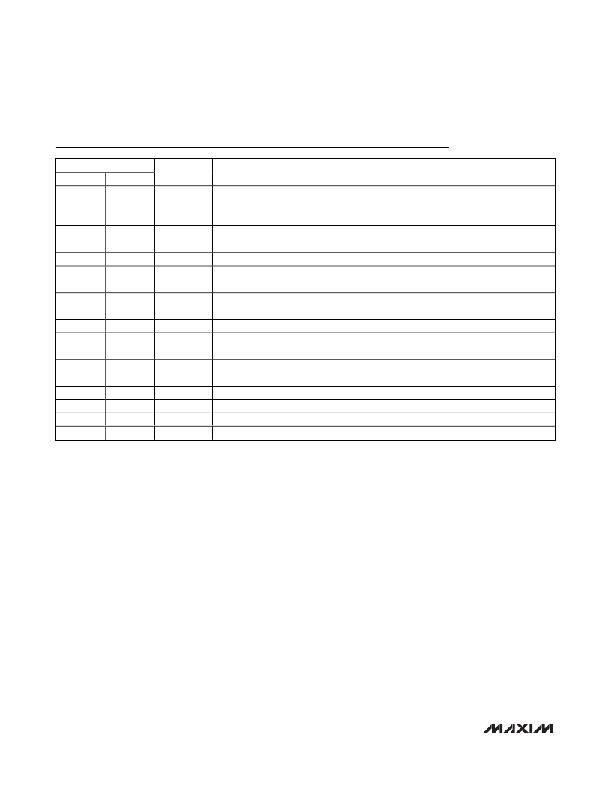
Pin Description
PIN
MAX7306 MAX7307
NAME
FUNCTION
Reset Input. RST is an active-low input, referenced to V DD , that clears the 2-wire interface,
1
1
RST
which can be configured to put the device in the power-up reset condition and reset the
PWM and blink timing.
2
3
4
5
6
—
7
8
9
10
—
2
3
4
5
6
7
—
8
9
10
—
P1/ INT
GND
P2/OSCIN
P3/OSCOUT
P4
V LA
AD0
V DD
SDA
SCL
EP
Input/Output Port. P1/ INT is configurable as an open-drain I/O or as a transition detection
interrupt output.
Ground
Input/Output Port. P2/OSCIN is configurable as a push-pull I/O, open-drain I/O, or as the
PWM/blink/timing oscillator input.
Input/Output Port. P3/OSCOUT is configurable as a push-pull I/O, open-drain I/O, or as
the PWM/blink/timing oscillator output.
Input/Output Port. P4 is configurable as a push-pull I/O or an open-drain I/O.
Port Supply for P1–P4. Connect V LA to a power supply between 1.40V and 5.5V. Bypass
V LA to GND with a 0.1μF capacitor.
Address Input. Sets the device slave address. Connect to GND, V DD , SCL, or SDA to
provide four address combinations.
Positive Supply Voltage. Bypass V DD to GND with a 0.1μF ceramic capacitor.
Serial-Data I/O
Serial-Clock Input
Exposed Pad (μMAX only). Connect to GND.
6
_______________________________________________________________________________________
发布紧急采购,3分钟左右您将得到回复。
相关PDF资料
MAX831EVKIT-SO
EVAL KIT FOR MAX831
MAX8513EVKIT
EVAL KIT FOR MAX8513
MAX8552EUB+
IC DRIVER MOSFET HS 10-UMAX
MAX8595XETA+T
IC LED DRIVR WHITE BCKLGT 8-TDFN
MAX8607ETD+T
IC LED DRIVR PHOTO FLASH 14-TDFN
MAX8608YETD+T
IC LED DRVR WT/OLED BCKLT 14TDFN
MAX8631XETI+T
IC LED DRVR WHITE BCKLGT 28-TQFN
MAX8645YETI+T
IC LED DRVR WHITE BCKLGT 28-TQFN
相关代理商/技术参数
MAX7307EVKIT+
制造商:Maxim Integrated Products 功能描述:MAX7307 EVAL KIT/EVAL SYS - Rail/Tube
MAX730A
制造商:MAXIM 制造商全称:Maxim Integrated Products 功能描述:5V, Step-Down, Current-Mode PWM DC-DC Converters
MAX730AC/D
功能描述:直流/直流开关转换器 DICE SALES DICE RoHS:否 制造商:STMicroelectronics 最大输入电压:4.5 V 开关频率:1.5 MHz 输出电压:4.6 V 输出电流:250 mA 输出端数量:2 最大工作温度:+ 85 C 安装风格:SMD/SMT
MAX730AC/D DIE
制造商:Maxim Integrated Products 功能描述:
MAX730ACPA
功能描述:直流/直流开关转换器 5V Step-Down DC/DC Converter RoHS:否 制造商:STMicroelectronics 最大输入电压:4.5 V 开关频率:1.5 MHz 输出电压:4.6 V 输出电流:250 mA 输出端数量:2 最大工作温度:+ 85 C 安装风格:SMD/SMT
MAX730ACPA+
功能描述:直流/直流开关转换器 5V Step-Down DC/DC Converter RoHS:否 制造商:STMicroelectronics 最大输入电压:4.5 V 开关频率:1.5 MHz 输出电压:4.6 V 输出电流:250 mA 输出端数量:2 最大工作温度:+ 85 C 安装风格:SMD/SMT
MAX730ACSA
功能描述:直流/直流开关转换器 5V Step-Down DC/DC Converter RoHS:否 制造商:STMicroelectronics 最大输入电压:4.5 V 开关频率:1.5 MHz 输出电压:4.6 V 输出电流:250 mA 输出端数量:2 最大工作温度:+ 85 C 安装风格:SMD/SMT
MAX730ACSA+
功能描述:直流/直流开关转换器 5V Step-Down DC/DC Converter RoHS:否 制造商:STMicroelectronics 最大输入电压:4.5 V 开关频率:1.5 MHz 输出电压:4.6 V 输出电流:250 mA 输出端数量:2 最大工作温度:+ 85 C 安装风格:SMD/SMT
